Comparative Study of Gamma Ray and Neutron Radiation on Some Electrical Properties of n-CdSe/p-Si Photodiodes.
Keywords:
Gamma-ray, neutron radiation, Photodiode , Irradiation, CdSeAbstract
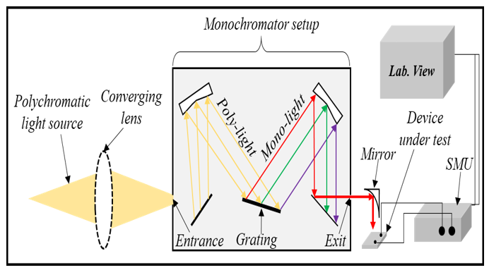
Cadmium Selenide (CdSe) thin films were prepared on silicon(p-type) substrates using the pulsed laser deposition technique (PLD). They were then annealed at 300 ºC for one hour to get diodes used as a visible light detector. Four diodes were subjected to four different intervals of gamma radiation emitted from the 226Ra source. For comparison, four of these diodes were subjected to four different intervals of neutron radiation using a ( 241Am -10Be) source; the other diodes were kept without exposure to irradiation. I-V measurements studied the electrical properties of these samples. Results of gamma-irradiated devices show that dark current decreases for the irradiated thin films. Forward current under illumination increases when exposed to small gamma radiation values and then decreases with higher exposure values. While the value of reverse current increases with the irradiation. The results of I-V characteristics for neutron irradiation devices show that the value of current under illumination increases when exposed to small values of neutron radiation, then it decreases with higher values of exposure. However, dark current decreases significantly with irradiation. The effect of the gamma and neutron irradiation was clear on the response/recovery period for all irradiated devices. However, it was more profound in the response/recovery time of pristine devices. Also, the photo-responsivity of the pristine device was larger than that of the irradiated devices, and it decreased with increasing absorbed doses of gamma and neutron radiation.
Downloads
References
Yadav, A. A., M. A. Barote, and E. U. Masumdar. "Studies on cadmium selenide (CdSe) thin films deposited by spray pyrolysis." Materials chemistry and physics 121.1-2 (2010): 53-57.
Shelke, Nitin T., S. C. Karle, and B. R. Karche. "Photoresponse properties of CdSe thin film photodetector." Journal of Materials Science: Materials in Electronics 31.18 (2020): 15061-15069.
Bao, Zheng, et al. "The study of CdSe thin film prepared by pulsed laser deposition for CdSe/CdTe solar cell." Journal of Materials Science: Materials in Electronics 27.7 (2016): 7233-7239.?
Ashry, M., and S. Fares. "Radiation effect on the optical and electrical properties of CdSe (In)/p-Si heterojunction photovoltaic solar cells." Journal of Semiconductors 33.10 (2012): 102001.
Oksuzoglu, Fatih, et al. "Structural properties of cadmium selenide nanowires prepared by chemical bath deposition for the electrical and photosensitive characteristics of the p-Si/CdSe heterojunction." Journal of Photonics for Energy 10.2 (2020): 025502-025502..?
Al Refaei, Duha H., Laith A. Najam, and Laith M. Al Taan. "The Effect of neutron irradiation on optical, structural and morphological properties of cadmium selenide thin films." J. Rad. Nucl. Appl 6 (2021): 207-16.
Mohammed, Hassan H., and Salwan KJ AL-Ani. "The Fabrication of the Infrared CdSe Doped With Cu Photodetector." Applied Physics Research 8.3 (2016): 96-103.
Kumara, Pawan, et al. "Effect of post-growth annealing process on optical properties of CdSe thin films on Si p-type substrate deposited by pulsed laser deposition technique." The International Journal of Analytical and Experimental Modal Analysis 13.6 (2021): 3016-3028.
Al Abbas, J. M., L. Al Taan, and M. M. Uonis. "Structural and optical properties of cadmium selenide thin film growth with different substrate temperatures by spray pyrolysis deposition." Chalcogenide Letters 20.12 (2023).
Choudhary, Ritika, and R. P. Chauhan. "Gamma irradiation induced modifications in spin coated CdSe thin films." Journal of Materials Science: Materials in Electronics 27.11 (2016): 11674-11681.
Jamil, Nawfal Y., et al. The Effect of ?-Irradiation on the Structural and Physical Properties of CdSe Thin Films. Diss. Sumy State University, 2013.
Rafik, Hazem, and Mahmoud Izerrouken. "Radiation damage induced by reactor neutrons in nano-anatase TiO2 thin film." Radiation Physics and Chemistry 177 (2020): 109114..
Hammo, Zainab, Laith Najam, and Laith Al-Taan. "Neutron Radiation Effects on the Performance of the CdSe Thin Film for Photodetector Applications." Trends in Sciences 21.11 (2024): 8541-8541.
Khatter, Jaya, and R. P. Chauhan. "Gamma-ray induced modifications on CdS nanorod mesh: Structural, optical, and electrical properties." Radiation Physics and Chemistry 182 (2021): 109353.
Sudha, A., T. K. Maity, and S. L. Sharma. "Effects of gamma irradiations on structural and electrical properties of indium oxide thin films prepared by thermal evaporation." Materials Letters 164 (2016): 372-375.
Kaleli, Murat, et al. "Studying the effects of thermal neutrons irradiation on CuInGaSe2 thin film." Journal of Madenat Alelem University College 12.2 (2020): 186-197.
Davidyuk, H. Ye, V. V. Bozhko, and L. V. Bulatetska. "Specific features of the effect of irradiation with electrons and neutrons on photoelectric properties of CdS single crystals nominally undoped and doped with Cu." Semiconductors 42.10 (2008): 1244-1248.
Najam, Laith, Laith M. Al Taan, and Duha Hashim Al Refaei. "Preparation and study of the physical properties of CdSe films deposited by a chemical bath method and exposed to neutron irradiation: Effect of neutron Irradiation on a CdSe film prepared." International Journal of Engineering and Applied Physics 4.1 (2023): 909-918.
Kumari, Manju, Pallavi Rana, and R. P. Chauhan. "Modifications in structural and electrical properties of gamma irradiated CdSe nanowires." Nuclear Instruments and Methods in Physics Research Section A: Accelerators, Spectrometers, Detectors and Associated Equipment 753 (2014): 116-120.
Ahmad, Shabir, et al. "Effect of gamma irradiation on the structural and optical properties of thin films of a-CdSe." Optik 126.23 (2015): 3501-3505.
Nikoli?, D., et al. "Effects of successive gamma and neutron irradiation on solar cells." Journal of Optoelectronics and Advanced Materials 17.3-4 (2015): 351-356.
Aly, K. A., A. Dahshan, and Y. Saddeek. "Optical properties of as-prepared and irradiated In–Cd–Se thin films." Journal of Materials Science: Materials in Electronics 33.16 (2022): 12663-12673.
Downloads
Published
How to Cite
Issue
Section
License
Copyright (c) 2025 zainab hamoo, Laith AL Taan, Laith Najam

This work is licensed under a Creative Commons Attribution 4.0 International License.
Copyright on any article in the International Journal of Engineering and Applied Physics is retained by the author(s) under the Creative Commons license, which permits unrestricted use, distribution, and reproduction provided the original work is properly cited.
License agreement
Authors grant IJEAP a license to publish the article and identify IJEAP as the original publisher.
Authors also grant any third party the right to use, distribute and reproduce the article in any medium, provided the original work is properly cited.
Similar Articles
- Funminiyi Oyekunle, Sanya OGUNSUSI, E.O. Aiyewalehinmi, Kunle AMOKO, Assessment of occupational health and safety risks in selected construction sites in oyo state, Nigeria , International Journal of Engineering and Applied Physics: Vol. 5 No. 1: January 2025
You may also start an advanced similarity search for this article.
Most read articles by the same author(s)
- Laith Al Taan, Samir Ahmad, Mixer Circuits Design and Performance Analysis using Planar Schottky Diodes – Simulation with MWO , International Journal of Engineering and Applied Physics: Vol. 4 No. 3: September 2024
- Zainab Hammo, Laith Najam, Laith Al_Taan, Gamma Radiation Effects on The Performance of The CdSe Thin Film for Photodetector Application , International Journal of Engineering and Applied Physics: Vol. 4 No. 2: May 2024
- Laith Najam, Laith M. Al Taan , Duha Hashim Al Refaei , Preparation and Study of the Physical Properties of CdSe Films Deposited by a Chemical Bath Method and Exposed to Neutron Irradiation , International Journal of Engineering and Applied Physics: Vol. 4 No. 1: January 2024
- Zainab Mowafaq Marie, Laith Najam, Taha Yaseen Wais, Berivan F. Namq, Radionuclides Distribution in Al-Qayyarah Oil Wells and refinery in Nineveh Government, Iraq , International Journal of Engineering and Applied Physics: Vol. 4 No. 3: September 2024